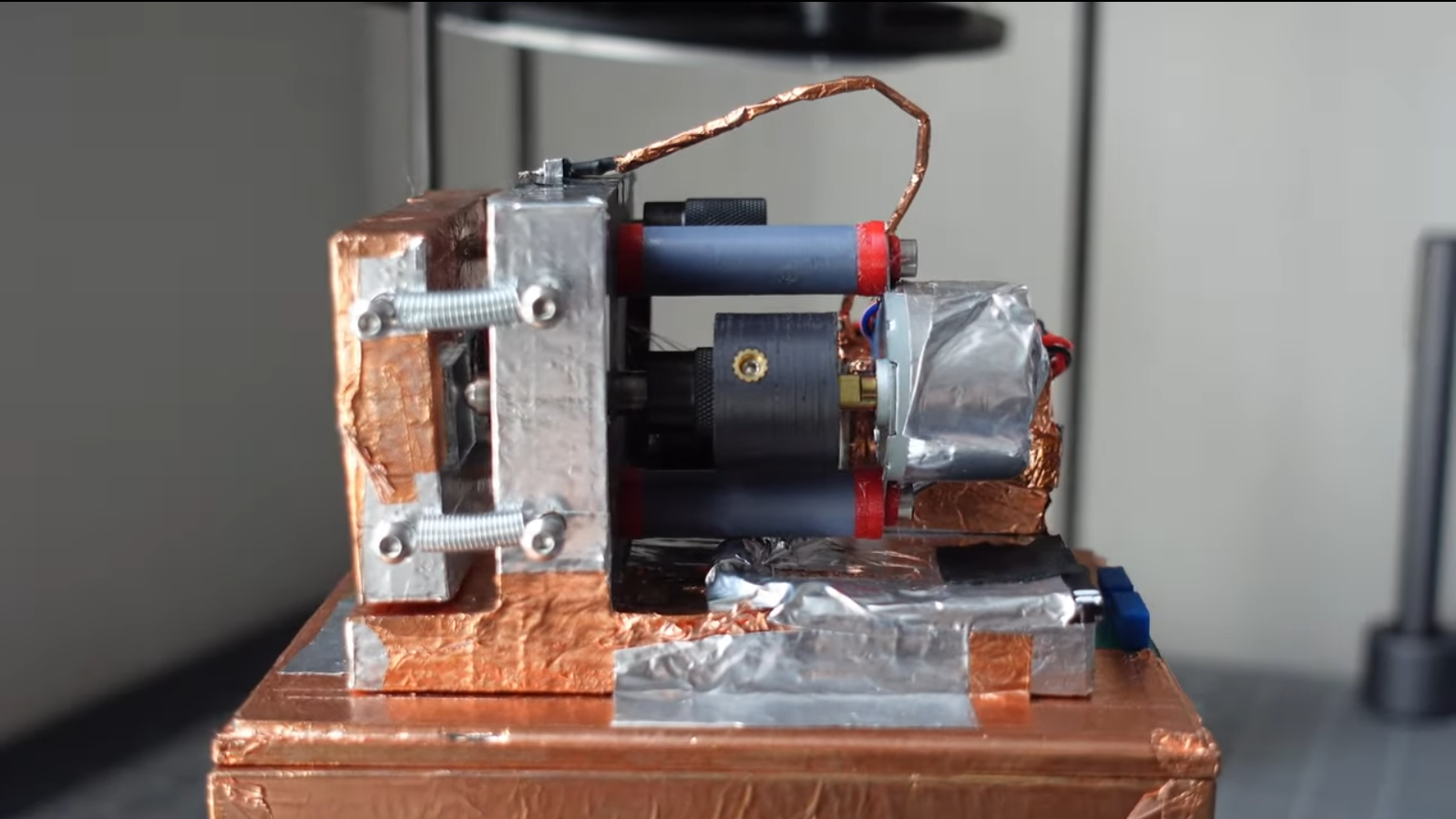
YouTuber [MechPanda] has recreated a DIY STM hack we covered about ten years ago, updating it to be primarily 3D-printed, using modern electronics, making it much more accessible to many folks. This simple STM setup utilises a piezoelectric actuator constructed by deliberately cutting a piezo speaker into four quadrants. With individual drive wires attached to the four quadrants. They (re)discovered that piezoelectric ceramic materials are not big fans of soldering heat. Still, in the absence of ultrasonic welding equipment, they did manage to get some wires to take to the surface using low-temperature solder paste.
They glued a makeshift probe holder on the rear side of the speaker actuator, which was intended to take a super sharp needle-like piece of tungsten wire. Putting the wire in tension and cutting at a sharp angle makes it possible with many attempts to get some usable points. Usable, in this instance, means sharp down the atomic level. The sample platform, actuator mount and all the connecting parts are 3D-printed with PA-CF. This is necessary to achieve enough mechanical stability with normal room temperature fluctuations. Three precision screws are used to level the two platforms in a typical kinematic mount structure, which looks like the only hard-to-source component. A geared stepper motor attached to the probe platform is set up to allow the probe to be carefully advanced towards the sample surface.

The next issue concerns vibration damping of the whole assembly. This was achieved with a simple hanging sprung platform, damped using an aluminium plate and magnets mounted underneath—a simple and effective eddy-current damper setup. For the electronics, a Teensy 4.1 runs the show, driving the four quadrants via a brace of AD5761 serial DACs and a few summing amplifiers. Three DACs generate the X, Y and Z signals, which are sent to the quadrants as Z+/-X and Z+/-Y, and the fourth DAC generates a sample bias signal. The tunnelling current picked up by the probe tip is first sent to a preamplifier constructed using a very high gain transconductance (current-to-voltage) amplifier. However, the part used was not identified. The whole assembly is electrically shielded with metallic tape, including the cable running down the main analog board, which hosts an LTC2326 ADC that can handle the bipolar differential signal being fed to it. The software was programmed using the Arduino stack for ease of use. The reason for the high-speed micro is the need to control the scanning signals based on the measured tunnelling current to form a control loop. We didn’t dig into precisely how that works! As can be seen from the video, they managed to get some quite decent images of the surface of a freshly peeled HOPG (graphite) lab specimen, so the setup works, and the noise sources are under control.
To read along, check out the project GitHub page, but more importantly, the original project by [Dan Berard.]
Thanks to [rolmie] for the tip!