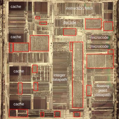
Whereas the CPUs and similar ASICs of the 1970s had their transistors laid out manually, with the move from LSI to VLSI, it became necessary to optimize the process of laying out the transistors and the metal interconnects between them. This resulted in the development of standard-cells: effectively batches of transistors with each a specific function that could be chained together. First simple and then more advanced auto-routing algorithms handled the placement and routing of these standard elements, leading to dies with easily recognizable structures under an optical microscope. Case in point an original (P54C) Intel Pentium, which [Ken Shirriff] took an in-depth look at.
Using a by now almost unimaginably large 600 nm process, the individual elements of these standard cells including their PMOS and NMOS components within the BiCMOS process can be readily identified and their structure reverse-engineered. What’s interesting about BiCMOS compared to CMOS is that the former allows for the use of bipolar junction transistors, which offer a range of speed, gain and output impedance advantages that are beneficial for some part of a CPU compared to CMOS. Over time BiCMOS’ advantages became less pronounced and was eventually abandoned.
All in all, this glimpse at the internals of a Pentium processor provides a fascinating snapshot of high-end Intel semiconductor prowess in the early 1990s.
(Top image: A D flip-flop in the Pentium. Credit: [Ken Shirriff] )
